Welcome to the website of the annual Francken Symposium! This year's theme will be 'Photovoltaics' with the slogan "Illuminating the Future". During this event speakers will deliver lectures about the physics behind the Photovoltaics and its possible advances in the future.
Photovoltaics have been a research topic for decades, however, over the past decade it has seen a remarkable evolution, characterized by rapid technological advancements, significant cost reductions, and a substantial increase in global installation capacities. The focus has been on enhancing the efficiency, durability, and manufacturability of solar cells and modules, alongside integrating them into a wide range of applications, from residential rooftops to large-scale solar farms and even wearable technology. With ongoing innovations and policy support, the future of photovoltaics appears bright, promising to play a pivotal role in meeting the world's growing energy needs while addressing climate change challenges.
As an organization, we welcome you to join us on the 21st of May 2024 for an exciting and informative day on the subject surrounded by experts in the field.
The price for attending is €7.50 for Francken members and €10.00 for non-Francken members. The first 110 spots are guaranteed, so sign-up fast! After these are gone attending might not be possible or it might be slightly more expensive.
Maria Loi
Jan Anton Koster
Energy Conversion
Peter van Arkel
Adriana Creatore
Dick Heslinga
Herman Duim
Dennis Francke
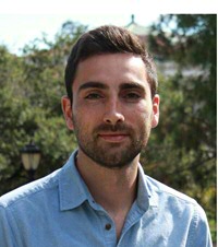
Maria Antonietta Loi studied physics at the University of Cagliari in Italy where she received the PhD in 2001 for a thesis on Photoexcitations and Interchain Interactions in Conjugated Oligomers and Polymers which was carried out in the group of Prof. G. Bongiovanni and A. Mura. In the same year she joined the Linz Institute for Organic Solar cells, of the University of Linz, Austria as a postdoctoral fellow. Later she worked as researcher at the Institute for Nanostructured Materials of the Italian National Research Council in Bologna, Italy. In 2006 she became assistant professor and Rosalind Franklin Fellow at the Zernike Institute for Advanced Materials of the University of Groningen, The Netherlands. She is now full professor in the same institution and chair of the Photophysics and OptoElectronics group.
She has published more than 240 peer-reviewed articles on photophysics and optoelectronics of different types of materials. The main interest is unravelling the properties of novel semiconductors and to tune their properties to fabricate highly performing optoelectronic devices (Solar cells, LEDs, Photodetectros etc.)
We use a combination of experimental and simulation techniques to identify how the performance of devices is related to the properties of the materials and basic physical processes. Our work focuses on functional materials that can be easily processed from solution. This means that using the materials to make a functional device requires little energy and is cheap.
Innovation in thin film and interface engineering has played an essential role in pushing the conversion efficiency of the most widespread photovoltaic (PV) technology, i.e. crystalline silicon-based (c-Si), towards its thermodynamic limit. In this respect, ultra-thin, conformal, high-purity Al₂O₃ thin films synthesized by ALD are key in c-Si PV manufacturing industry as they passivate the c-Si surface, thereby suppressing a major channel of electron-hole pair recombination. Recently, we have explored the ALD synthesis of thin films for metal halide perovskite- based photovoltaics. The latter has rapidly reached a conversion efficiency of 26% and, when coupled with c-Si PV in a so-called tandem device, leads to efficiencies already beyond 33%. In this contribution I will discuss the merits which ALD offers to perovskite-based PV by reviewing our work on NiO-based hole transport layers and discussing in depth the case study of ALD SnO 2 . The latter is implemented in perovskite PV R&D and industry as buffer layer, i.e., imparting thermal and environmental stability to the device, while protecting the perovskite absorber and fullerene electron transport layer from the sputtering of the transparent top contact. More recently, ALD SnO 2 is explored as solvent barrier layer in the tunnel recombination junction of perovskite/perovskite tandem PV, to prevent the damage of the wide-gap perovskite absorber when processing the narrow band-gap perovskite cell. Although we can conclude that several ALD merits are already extensively acknowledged by the PV community, studies addressing ALD film growth on challenging substrates such as fullerenes and metal halide perovskites are rarely reported in literature. We are convinced that these studies provide a rationale to implement more efficiently these layers at device level and promote process upscaling. Therefore, this contribution will also highlight the adoption of in situ diagnostics, namely spectroscopic ellipsometry and IR spectroscopy, to characterize the ALD SnO 2 growth on two commonly adopted fullerenes, C60 and [6,6]-phenyl-C61-butyric acid methyl ester (PCBM). Our studies show that a substrate-inhibited growth occurs in the case of PCBM and, to a minor extent, in the case of C60, with respect to the traditional c-Si substrate. Moreover, IR spectroscopy highlights the loss of vibrational features of the ester group in PCBM upon SnO 2 growth, whereas C60 is chemically unaffected. We conclude that the the delayed film growth and chemical modifications detected on PCBM are responsible for the consistently lower device performance when ALD SnO 2 is grown on PCBM instead of C60.
The current energy and climate challenges make the transition to a sustainable and renewable energy model increasingly necessary. Solar energy conversion through the development of efficient solar cells is a promising solution. As the materials used in solar cells play a crucial role in determining their performance, materials science, combining disciplines such as physics, chemistry and engineering, assumes a crucial position in driving advancements in this field.
In this talk, we will discuss the fundamental principles behind solar cells, exploring their structure, fabrication methods, key challenges, and ongoing research efforts aimed at addressing these challenges from a materials science point of view. We will highlight our latest advancements in the development of transparent electrodes and contact layers for solar cells and vacuum-deposited halide perovskites for application in photovoltaic technologies.
In the first part of the talk, we focus on the recent developments on transparent electrodes and contact layers for high efficiency solar cells. Specifically, we discuss how the microstructure of the transparent conductive oxide (TCO) impacts the electronic properties of hole selective contact layers for perovskite solar cells, using the case example of Sn-doped In 2 O 3 (ITO) and self-assembled monolayers (SAMs).
In the second part, we'll shift our attention to the growth of metal halide perovskites for solar cells, with a particular focus vacuum-based deposition of these perovskites. We'll discuss the potential of Pulsed Laser Deposition (PLD) as an alternative vacuum, vapor-based deposition technique for precisely tailoring complex metal halide perovskite thin films. We will also discuss recent development on the fabrication of perovskites by hybrid vacuum and solution processes. All this with the motivation of future application in perovskite-based tandem devices.
These advancements represent crucial steps towards controlling growth processes and ensuring the future scalability of materials used in efficient photovoltaic devices.
Transforming the steady progress in photovoltaics Research and Development into succesful industrial initiatives is of prime importance for the health of the sector in Europe, but over the last decade has proven extremely challenging. Ever increasingly, the mainstream of PV manufacturing worldwide is shaped by multi-GW scale, commodization, ultra-low cost, and a relentless pace of innovation. Yet, in face of these formidable barriers to entry, but recognizing the strategic imperative of energy sovereignity, this is the time that EU policy is shaping up to do ‘whatever it takes’ to favour the launching of a new generation of industrial PV manufacturing companies across the Si PV value chain. Taking a selective look at current innovation trends, the colloquium will identify promising technologies and industrial strategies. We will analyze the dynamics at work, the difficulties encountered, and the factors for success. Concrete cases of industrial initiatives will be placed in the broader EU policy context and in the specific strategy of the Netherlands via the ‘SolarNL’ Groeifonds programme. Will the renaissance succeed? Much to be done, much to be won.
Photonic Integrated Circuits (PICs) are revolutionizing optical devices in a similar way as the electronic IC has done for computing. Lasers, detectors, modulators and waveguides are all integrated into a single chip. This integration reduces cost, power consumption, size and weight. These advantages of PICs are game changers in applications like autonomous vehicles, healthcare, agrifood, datacenters and artificial intelligence.
In his talk Peter will take you on a journey through the evolution of PICs, the current applications, and future trends to contribute to more sustainable world.
Delmic is a passionate high-tech company based in Delft, Netherlands that develops powerful and user-friendly solutions for electron microscopy, bringing life science and material science researchers and organizations closer to research insights across diverse application fields.
Abstract talk by Herman Duim, application specialist for Cathodoluminescence at Delmic: Understanding the fundamental properties of materials is essential for the advancement of technology. In both academic and industrial research, characterization plays a pivotal role, especially in the study of photovoltaic materials. Cathodoluminescence imaging represents a sophisticated technique that merges electron microscopy with light microscopy, offering unique insights. This talk introduces the basic principles of cathodoluminescence spectroscopy and illustrates its practical application in photovoltaic research through relevant examples. Join us as we explore how this advanced imaging method contributes to a deeper understanding of photovoltaic materials.
These days, a small USB stick costing only €10 can hold up to 16 GB of data. In hospitals, a camera the size of a pill can be swallowed to survey a patient's intestines. Modern pacemakers, critical devices that control abnormal heart rhythms, are now less than a tenth the size of earlier ones. And in the oceans, tiny GPS transmitters track endangered turtles to help protect them.
While these devices are incredibly small, they represent a big milestone in technological progress. At the heart of each of these life-enhancing innovations is a microchip a tiny package of integrated circuitry that powers the performance of the device.
In a world in which major breakthroughs measure only a few nanometres in size, the constant quest is to produce chips that are smaller, faster, more effective and less expensive. One of the major high-tech players leading the quest is ASML, a manufacturer of lithography systems for producing computer chips.
In a world that is becoming increasingly faster, more unpredictable and full of possibilities, Thales has great ambitions: to make your life better and safer! With a team of 80,000 strong in 68 countries, we are one of the largest high-tech employers in Digital Identity & Security, Transportation, Space, Defence & Security and Aerospace. About 2500 of our colleagues work in the Netherlands, divided over four cities: Huizen, Delft, Eindhoven and Hengelo (HQ).
Together with our knowledge partners, customers and suppliers, we work on radars for naval vessels, cyber security solutions, transport systems, communication equipment for the army, cryogenic cooling solutions and research & development for radar technology (in collaboration with TU Delft). This means we play a leading role in digital transformation, focusing on artificial intelligence, big data & data analytics, connectivity, mobility plus the internet of things and cyber security.
KIVI (The Royal Netherlands Society of Engineers) is the largest engineering association of the Netherlands. Engineers are fully committed to improving the quality of life in our society with their indispensable knowledge and technological solutions for societal problems. KIVI helps them with this. All engineering disciplines are represented within KIVI.
KIVI has a growing international community of engineers from all over the world working in the Netherlands. For those engineers we have the international community pages, with information about English language activities, news, and their home-base KIVI-section: KIVI International Engineers.